Answers to those Doggone Thermal Design Questions
By Tony Kordyban
Copyright by Tony Kordyban 2002
Dear Mr. Everything Wrong,
I have heard your criticism of the use of Theta j-a, the so-called thermal resistance from junction to ambient. You argue that it is not good for estimating the junction temperature of a component, for a variety of reasons, and I agree with you. But what about that other thermal resistance, Theta j-c, the resistance between the junction and the case? Is that number more accurate, or at least, more useful than Theta j-a? Can I use it to estimate the junction temperature of a component after I have measured the case temperature (assuming that I know the power dissipation)?
I thought that Theta j-c should be better for two reasons:
1. Unlike for Theta j-a, I know where to measure the case temperature, but the “ambient” air temperature referenced by Theta j-a is not defined.
2. Theta j-c is the conductive resistance inside the package, which depends only on the materials from which it is made, so it doesn’t change.
I am hoping that even if Theta j-c is not totally accurate, it will at least be conservative. By conservative I mean that it will give me an estimate of junction temperature that is never lower than the actual junction temperature. If there is error, it should estimate too high, so that I don’t approve a component for use, and then have it fail thermally in the field.
Can you help me understand Theta j-c better?
Buffaloed in up-stateNew York
Dear Buff,
Here is the short answer to your question:
- Theta j-c is not any better at estimating junction temperature than Theta j-a.
- Theta j-c is not just a function of the construction and materials of the component package. It also depends on the Printed Circuit Board (PCB) to which it is soldered, among other factors, so it will change from application to application.
- Theta j-c is not guaranteed to give you a conservative estimate of junction temperature. In some cases it will give you a junction temperature estimate lower than the actual value.
Don’t you feel better already?
Let’s define what you really need, and then let’s define Theta j-c, so we can see how they are not the same thing.
What you want: It is simple to attach a thermocouple to the surface of a component. That is pretty close, but not quite close enough to the temperature we all lust after — the temperature of the chip itself (also called the die or junction.) How much hotter is the chip than the case (the outside surface of the component package)? Naturally that depends on the heat dissipated by the chip. It would be nice if there were some characteristic number for any component package, that could tells us the temperature difference between the chip and the case, assuming we know the power of the chip. The formula for that might look like this:
Tj – Tc = package characteristic x Power
What you get: That was the motive, I suppose, behind the creation of Theta j-c a long time ago. Here is how it is defined:
Theta j-c = (Tj – Tc) / Qt
| where | Tj | is the junction temperature |
| Tc | is the case temperature | |
| Qt | is the total heat from the chip |
It is measured by mounting a component on a standard test board (about 4 in by 5 in). Qt, Tc and Tj are measured in a special chamber (sometimes in a liquid bath!) and Theta j-c is calculated. This sounds a lot like what you want, because
Tj – Tc = Theta j-c x Qt
Doesn’t that qualify Theta j-c to be the package characteristic you want?
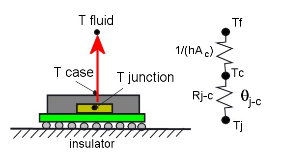
Well, not exactly. The only situation where this is really valid is shown in Figure 1.
If the component is mounted on a perfect insulator, then all the heat flows from the chip to the top of the package. There is only one path for heat to get to the surrounding fluid, and so that path can be characterized by a single resistance, which you could call Theta j-c, if you wanted to.
Even if Theta j-c were measured this way, it would not be very useful to you, because you are going to attach the component to a PCB, which is a pretty good heat spreader. And that changes everything.
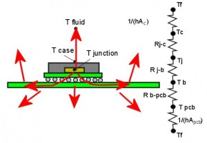
Package testers have to hook up the leads of their components somehow, too, so they use a PCB when they measure Theta j-c. It looks more like Figure 2.
As soon as you have a PCB, heat flows out of the chip through multiple paths, each with its own thermal resistance. Some heat still flows through the top surface, but lots of heat goes out through the leads, spreads in the PCB, and from there into the surrounding fluid.
To keep our story simple, let’s say that for our particular component there are only two heat paths — one up to Tc on the top surface, and the second down to the bottom of the package, where the leads connect to the PCB. I call the temperature at the bottom of the package Tb. If we included all the other heat paths, the argument would be the same, but much more complicated to follow.
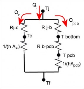
When you have two paths for heat to follow, the total chip heat is going to split up. Some will flow up to Tc, and the rest to Tb. How it splits depends on the relative resistances of the two paths. This kind of problem is usually attacked by drawing a resistor network, like in Figure 3.
I am going to use the letter R as a symbol of a true thermal resistance, which depends only on the dimensions and the material properties of the conduction path. Theta is not really a resistance — it is intended as a “figure or merit” for
comparing one kind of package against another.
Figure 3 is a resistor network for a component package soldered to a PCB. It has two parallel paths from the chip to the fluid. Below is an explanation of the symbols in the figure.
| Tj | junction temperature |
| Qc | the portion of the total chip heat that travels up through the top of the package |
| Qpcb | the portion of the heat that travels through the leads into the PCB |
| Rj-c | conduction resistance between the chip and the top of the package. This value is a constant for the package, because it depends only on the dimensions and materials of the package itself |
| h | the convective heat transfer coefficient between the solid surfaces and the surrounding fluid |
| Ac | the surface area of the top of the package. Together with h, it determines the thermal resistance between the case and the fluid, which is not a constant property of the package |
| Rj-b | the conduction resistance between the die and the bottom of the package |
| Rb-pcb | the spreading resistance from the leads throughout the PCB |
| A pcb | the surface area of the PCB (both sides) exposed to the fluid |
Even without writing out all the equations for solving this network, you can see that Tj is a function of ALL these variables. Most of them are nearly impossible for somebody like you or me to figure out for any real component on a real PCB. Look at the resistor network in Figure 3 and imagine that you can figure out Tj by just measuring Tc and knowing the total power and Theta j-c. That is equivalent to claiming you can calculate the current in any net in a circuit by measuring the voltage at one node, and knowing the total power and the overall impedance of the circuit.
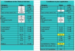
That is just a “hand-wavy” argument. Maybe numerically, Theta j-c is still good enough. So to figure that out I have put together the equations of the network into a spreadsheet. You can download it and plug numbers into it
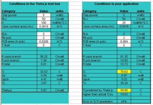
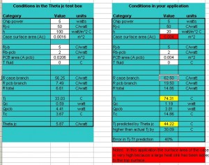
and see how good a job Theta j-c does at predicting Tj in your application. Here are some examples that I made for illustration. (Don’t bother clicking on the images of the spreadsheets — they are just screen captures. To change the values you’ll have to download the spreadsheet and run it on your machine.) Be aware that I have made up the resistance values out of whole cloth and they don’t represent any real component package.
One reason Theta j-c is not all that useful is that it is measured under different conditions than you will have in your application. In the Theta j-c test, the component and PCB are submerged in liquid. That’s why on the left side of the spreadsheet I chose a value for h of 100 W/m2C. Your air-cooled PCB has h closer to 20 W/m2C. The other big difference is that in the Theta j-c test, the component is all alone on a PCB with a large surface area. Your PCB may be even larger than the test PCB, but your component has to share all that area with bunches of
other components. So the effective area that can be used by your component to dissipate heat is probably much smaller.
In Figure 4 I made Rj-c much larger than Rj-b, and that leads to a value of Theta j-c that does a very poor job of predicting Tj in a more realistic application. The temperature rise between junction and case is off by over 19 degrees C. And Theta j-c predicts Tj to be lower than it actually is. So at least in theory, Theta j-c is NOT guaranteed to be conservative.
But it is not always wrong in the same direction, as you can see in Figure 5.
In Figure 6 I have added a large heat sink to the top of the component. That is included in the spreadsheet by
changing the surface area of the top (Ac) to a large number. I was a little surprised to see that, at least for this combination of resistances, adding a heat sink magnifies the error that Theta j-c has in estimating Tj. The heat sink causes more heat to flow through the top surface path, increasing the temperature rise between junction and case. The heat sink does reduce Tj, but not as much as you might think if you trusted in Theta j-c.
I don’t know how realistic my resistance values are. I have not investigated this very thoroughly, but just played around a little to see what happens. I invite you to do the same, especially if you might know some real values you can plug in. But I think I have demonstrated that it is not very hard to find combinations of resistances that make Theta j-c look bad.
After you’re done playing, you’ll be convinced that Theta j-c is not an accurate, or even a safe, way to estimate Tj. So how should you find Tj from a measurement of Tc?
I’m afraid that is an entirely different question, and you only get one question per month.
DOWNLOAD THE THETA J-C SPREADSHEET
—————————————————————————————————————
Isn’t Everything He Knows Wrong, Too?
The straight dope on Tony Kordyban
Tony Kordyban has been an engineer in the field of electronics cooling for different telecom and power supply companies (who can keep track when they change names so frequently?) for the last twenty years. Maybe that doesn’t make him an expert in heat transfer theory, but it has certainly gained him a lot of experience in the ways NOT to cool electronics. He does have some book-learnin’, with a BS in Mechanical Engineering from the University of Detroit (motto:Detroit— no place for wimps) and a Masters in Mechanical Engineering from Stanford (motto: shouldn’t Nobels count more than Rose Bowls?)
 In those twenty years Tony has come to the conclusion that a lot of the common practices of electronics cooling are full of baloney. He has run into so much nonsense in the field that he has found it easier to just assume “everything you know is wrong” (from the comedy album by Firesign Theatre), and to question everything against the basic principles of heat transfer theory.
Tony has been collecting case studies of the wrong way to cool electronics, using them to educate the cooling masses, applying humor as the sugar to help the medicine go down. These have been published recently by the ASME Press in a book called, “Hot Air Rises and Heat Sinks: Everything You Know About Cooling Electronics Is Wrong.” It is available direct from ASME Press at 1-800-843-2763 or at their web site at http://www.asme.org/pubs/asmepress, Order Number 800741.
